Our Aim
To provide you with an overview on New And existing technologies, hopefully helping you understand the changes in the technology. Together with the overviews we hope to bring topical issues to light from a series of independent reviewers saving you the time And hassle of fact finding over the web.
We will over time provide you with quality content which you can browse and subscribe to at your leisure.
TekSpek 's

NVIDIA GTX 750Ti Graphics Card
Date issued:
Something really new
After much speculation Nvidia's Maxwell architecture has finally arrived with the launch of two mainstream GPUs - the GeForce GTX 750 and GTX 750 Ti. Designed to drive a solid 1080p (1,920 x 1,080) gaming experience the new Maxwell-based GTX 750 and GTX 750 Ti cost a middling $119 and $149, respectively. Let's take a dive into the building blocks of the new GTX 750 Ti and see what makes it tick.
GTX 750 Ti
|
GTX 650
|
GTX 650 Ti
|
GTX 650 Ti Boost
|
|
| Die Code name | Maxwell GM107 |
Kepler GK107 |
Kepler GK106 |
Kepler GK106 |
| DX API | 11.1 |
11.1 |
11.1 |
11.1 |
| Process (nm) | 28 |
28 |
28 |
28 |
| Transistors (bn) | 1.87 |
1.30 |
2.54 |
2.54 |
| Die Size (mm²) | 148 |
118 |
221 |
221 |
| SM Units | 5 |
2 |
4 |
4 |
| Processors | 640 |
384 |
768 |
768 |
| Texture Units | 40 |
32 |
64 |
64 |
| ROP Units | 16 |
16 |
16 |
24 |
| L2 cache (KB) | 2,048 |
256 |
256 |
256 |
| GPU Clock (MHz) | 1,020 (1,085) |
1,058 |
928 |
980 (1,033) |
| GFLOPS | 1,389 |
812.5 |
1,425 |
1,587 |
| Texture fill rate (GT/s) | 43.4 |
33.9 |
59.2 |
66.1 |
| Memory Clock (MHz) | 5,400 |
5,000 |
5,400 |
6,008 |
| Memory Bus (bits) | 128 |
128 |
128 |
192 |
| Max Bandwidth (GB/s) | 86.4 |
80 |
86.4 |
144.2 |
| Power Connectors | None |
None |
6-pin |
6-pin |
| TDP (watts) | 60 |
64 |
110 |
134 |
| GFLOPS per watt | 23.15 |
12.92 |
12.92 |
10.75 |
| SLI | No |
No |
No |
Yes, 2-way |
| Current MSRP ($ USD) | 149 |
109 |
129 |
149 |
The focus of this TekSpek is on the faster flagship part, the GTX 750 Ti. This new Nvidia GPU is designed to tackle the ageing GTX 600-series trio of the GTX 650, GTX 650 Ti and GTX 650 Ti Boost. In specification terms the GTX 750 Ti resembles its GTX 600-series namesake the closest. They both share a similar memory configuration, level of compute and price point, although the GTX 750 Ti looks considerably slower on paper.
Yet do not be fooled by the numbers. The Maxwell-based GTX 750 Ti is not like-for-like comparable with the Kepler-based GTX 650 Ti (Boost). This plays out in performance as Nvidia claims the GTX 750 Ti is not only 25 per cent faster than the GTX 650 Ti, but also boasts a 30 per cent smaller die and half the total power consumption.
The wizardry would not be possible without the ground-up architecture redesign that is Maxwell. Nvidia's latest and greatest architecture learns from all the inefficiencies of its predecessor and adds some nifty new features of its own. The GTX 750 Ti is the first-generation implementation of an architecture that will likely be rolled out to higher-end models later on this year.
Maxwell: a better fit for the mainstream
Nvidia's desktop Maxwell roll-out starts with the volume mainstream segment, which is a financially shrewd decision by Nvidia. For the enthusiast it's a little deflating that high-end Maxwell is still some way off but it shouldn't be unexpected; Nvidia sells significantly more sub-$150 GPUs than $500 ones.
Maxwell is tailored for the mainstream market in a few ways. Firstly, Nvidia is able to achieve a dramatic 30 per cent die-size reduction without shrinking the established 28nm process. The fact this die-shrink is able to produce a GPU of comparable performance to its Kepler predecessor is even more noteworthy. Secondly, Maxwell is able to comfortably halve the power-draw figure of its predecessor. This makes the GTX 750 Ti a more suitable candidate for a wider variety of systems, especially OEM PCs, but it also reduces the cost of production since fewer, or lower-rated, power components can be used.
All of the above is well and good, but why is Maxwell so much more efficient and powerful than Kepler? Let's find out.
Why Maxwell is better
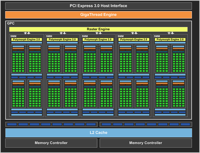
Shown above is an overview of the complete GM107 GPU used in the GTX 750 Ti. The basic structure is similar to Kepler in that the setup engine feeds the graphics processing cluster (GPC) that connects to a cluster of render outputs and passes out to the card's memory. This is normal architecture planning for a modern GPU.
The key difference between Maxwell and Kepler is the overall design of the GPC. Maxwell integrates five streaming multiprocessors (SMs) into each GPC compared to three within Kepler. Each SM has shrunk in size making use of 128 cores instead of the previous 192. This results in a overall GPC size of 640 for Maxwell compared to 576 for Kepler. Said reduction in cores for each SM allows Nvidia to boost per-SM efficiency.
Improving the shader units
Nvidia reveals that '...the SM scheduler architecture and algorithms have been rewritten to be more intelligent and avoid unnecessary stalls, while further reducing the energy per instruction required for scheduling.' The implication here is that Kepler's SM scheduler was likely inefficient at dealing with 192 cores, hence the transition to a smaller number of cores per SM.
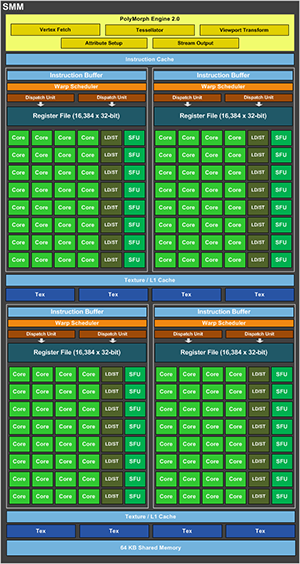
Maxwell's SMM blocks are not merely smaller replicas of Kepler, either. In Maxwell the SMM units are effectively split into four sub-SM units. Each SMM has four instruction buffers, register files, dispatch units and schedulers. Kepler made use of a single, larger version which was more space and power inefficient.
Zooming further into the microscope we can see that Nvidia has combined the texture and L1 caches into one, and these were separated on Kepler. In reverse the 64KB of share memory is now separated from the L1 cache. The ratio between cores and texture units has been reconfigured to 16:1, down from 12:1 on Kepler, resulting in decreased texturing ability.
To further enhance efficiency Nvidia has offset part of the scheduling duty to the GeForce driver, meaning less hardware needs to be present. This saves space on the die and decreases power consumption of the GPU.
The end result of all Nvidia's tinkering is that a Maxwell SMM is capable of 90 per cent of the performance of a Kepler SMX, despite possessing fewer cores, using less space and consuming less power. In theory, the Maxwell architecture allows Nvidia to cram in more SMs for a given silicon size, and that's how it achieves higher performance.
Excess power consumption has been trimmed in other ways, too. A boost in L2 cache size from 256KB to 2,048KB, an eightfold increase, reduces the number of access requests to the system memory thus reducing power consumption.
Those significant changes are largely implemented on the front-end of the GPU since that is where the biggest gains can normally be had. The back-end - ROPs, memory controller, etc. - is largely similar to Kepler's implementation. The GTX 750 Ti makes use of a pair of 64-bit memory controllers linked to 16 ROPs which should limit performance, although, the increased L2 cache and larger frame-buffer counter the effects of the narrow memory bus.
Video improvements
Nvidia has also used Maxwell as a springboard to redesign its NVENC video engine. The baked-in video-processing block now provides 2X faster encode and 8X faster decode performance compared to Kepler. Power efficiency has been increased here as well. A new decoder cache reduces memory access requests and a low power state called GC5 minimises GPU power consumption when running basic tasks like video playback.
Summary
Nvidia's Maxwell represents a leaner and more efficient variant of Kepler. A major overhaul of the SMM units, redesigned scheduling and power consumption tweaks make Maxwell the most power efficient desktop GPU architecture available. The persistent focus on improving performance-per-watt metrics mean Maxwell is ideal for TDP-limited environments like compact form factor PCs and notebooks.
Overall, Maxwell offers equivalent performance to Kepler with half the power budget. More importantly for the high-end desktop user this means twice the performance for the same power budget, relevant for when Nvidia releases another 250W flagship part. Of course this doesn't even factor in the effects of a process shrink down to 20nm, which would bring additional performance and power consumption benefits.
In summary, the Maxwell architecture underpinning the GeForce GTX 750 and GTX 750 Ti GPUs is more energy efficient and powerful than the Kepler design present in almost all other Nvidia GPUs today. As always, Scan Computers is stocking a wide selection of GeForce GTX 750 and GTX 750 Ti cards from today.