Our Aim
To provide you with an overview on New And existing technologies, hopefully helping you understand the changes in the technology. Together with the overviews we hope to bring topical issues to light from a series of independent reviewers saving you the time And hassle of fact finding over the web.
We will over time provide you with quality content which you can browse and subscribe to at your leisure.
TekSpek 's

NVIDIA GeForce GTX 480 / 470 architecture
Date issued:
What is NVIDIA Fermi?
Fermi is the current codename that's attributed to NVIDIA's next-generation GPU (Graphics Processing Unit) architecture. Physical cards will be released under the GeForce GT 400-series branding from March 26, 2010, and the initial batch of cards will target the enthusiast and high-performance segment of the market.
Fermi, or GF100, then, is the successor to the current GeForce GT 200-series range - currently headlined by the GeForce GTX 295 - that can be traced back to the GeForce GTX 280, launched in November 2006. So why the three-year-plus wait?
What makes Fermi tick?
Here's a high-level look at the NVIDIA's new graphics architecture. The sheer complexity of the chip means that the GPU is made up of some three billion transistors - the biggest to date - and will be fabricated on the 40nm process from TSMC.
Basing thoughts on previous high-end GPUs from NVIDIA and arch-rival AMD, Fermi's vital statistics mean that it won't be a cheap GPU to manufacture. A large die-size and, we suspect, low initial yields will ensure that pricing of first-run cards will be £400-plus, and possibly significantly higher for the range-topping model.
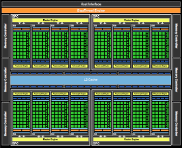
Financial considerations aside, Fermi's layout is new and highly modular. In its best form, GF100, as shown above, will be composed of four GPCs (Graphics Processing Clusters), which can be thought of as mini-GPUs themselves.
Mini GPUs
Each GPC contains four Streaming Multiprocessors (SM) that are composed of 32 cores each, leading to a per-GPC count of 128 and a card-wide tally of 512. This compares favourably with the incumbent GeForce GTX 285's 240 cores. As a strategic shift in thinking, the GPCs also contain their own setup engine, on-chip cache, and texture units.
The reason NVIDIA has chosen to design mini-GPUs rather than a fixed top-to-bottom setup lies with the innate complexity in keeping 512 cores efficiently fed with data. Having mini-GPUs breaks down that complexity into easily-manageable chunks and should pave the way for future NVIDIA designs that increase the processing cores to 1,000-plus.
DX11 and the tessellator
Impressing upon the point of efficient architecture via modularity, the Fermi GPU is a DX11 card that also features hardware-based tessellation "the ability to generate complex, many -triangle models from low-detail inputs" whose production would otherwise heavily tax other card resources.
Fermi's modular, per-GPC 'Polymorph Engine' is better suited to handling the output when compared with a single global (card-wide) setup, NVIDIA says. The proof of such a claim will be examined when tessellation performance is evaluated once the GPUs are reviewed.
Flexible caches
NVIDIA has also designed Fermi to keep as much data on the GPU as possible. Much like a CPU, the on-GPU caches work at a considerably faster rate than GPU-connected memory. To this end, Fermi increases L2 cache "the light-blue section in the middle of the picture" from 256KB to a unified 768KB and also introduces a configurable cache of 64KB per SM.
Interestingly, this can be split 16KB/48KB and broken down into shared/L1 cache and vice versa. The larger on-chip caches also mean that Fermi is in a better position to handle something like raytracing, where light-rays need to be calculated on-the-fly through constant accesses to chip memory, as the next set of compute isn't known beforehand.
Back-end and memory-controller
As NVIDIA has designed to keep as much communication on the GPU as possible, the back-end is significantly improved when compared to GeForce GT 200. The ROPs (raster back-ends) now number a maximum of 48 and are grouped in six partitions of eight (dark-blue, just behind the L2 cache) and, NVIDIA claims, have increased filtering performance due to better colour compression, where 8x AA application takes a minor performance hit when compared to traditional 4x AA.
Launched with the GeForce GTX 280, coverage sample antialiasing (CSAA) is NVIDIA's attempt to provide greater AA precision through an efficient computational cost. CSAA is now improved in GF100/Fermi with the ability to run 24 samples per pixel (in addition to the eight 'proper' MSAA samples). NVIDIA's new technique allows for 32 samples and 33 levels of transparency, enabling 'sharp-edge' objects to better blend in with their surroundings.
The ROPs then link out to the memory-controller, just as in any GPU design, but this time to six partitions that are 64 bits wide. What this means is that GF100 has a narrower memory width than GeForce GT 200, which was 512 bits, yet it should be offset by the use of high-speed GDDR5 RAM. Clearly, the balance of resources has shifted in favour of keeping as much as possible on the GPU - a common theme.
Compute machine
As much of a general-purpose computer as a GPU, the parallel architecture is also designed for the high-performance computing segment in mind. The enhanced cache structure, detailed above, helps with general computations, and Fermi's adherence to the IEEE 754-2008 floating-point standard means that it can run high-accuracy tests (double-precision support) at an increased rate when compared to anything NVIDIA has designed before.
Fermi also supports a range of programming models from C and C++ CUDA to OpenCL, PhysX and OptiX RayTracing. NVIDIA hopes to encourage a greater number of developers to use its new 'compute machine' for solving complex calculations.
Architecture summary and probable performance for Fermi
NVIDIA's Fermi marks a significant change in how the company sees the design of GPUs. Fundamentally different to incumbent GeForce GT 200 by now having up to four 'mini-GPUs' instead of the fixed top-to-bottom arrangement, NVIDIA hopes to increase overall GPU efficiency, both for games and general-purpose calculation, by allocating resources in what it thinks is a more-balanced approach. In one sense, the range-topping model can be thought of, somewhat tenuously, as a four-way SLI card.
The modular approach also dictates exactly how the company will trim the GPU down to fit into different segments. The ultra-high-end design will carry the four GPCs, as per the diagram. The high-end model will do away with a GPC, we imagine, the mid-range with another, and the low-end will only have one, it is reasonable to assume.
Fermi, it appears, has the attributes to be a very fast gaming card and, just as importantly, efficient for non-graphics workloads. NVIDIA's main problems will stem not from the design, which is decent, but from being able to bring enough physical GPUs up to a passing grade - remember the 3bn+ transistors? - whereby they can be sold to the general public.
The actual cards - GeForce GTX 480 and GTX 470
We now know that there will be two cards based on the GF100 Fermi architecture at launch. GeForce GTX 480 is the faster of the two and will be composed of 480 cores rather than the 512 prescribed by the architecture. This means that NVIDIA will switch off one stream-processing unit that's made up of 32 cores. The reason for doing this appears to lie with ensuring that production yields are decent enough to make the GPU economically viable.
GeForce GTX 480 will be clocked in at 700MHz core, 1,400MHz shader, and have 1,536MB of GDDR5 memory operating at 3,696MHz. The numbers aren't all that impressive considering what AMD has released last year, but it's the highest clocks that NVIDIA feels confident in guaranteeing without running into thermal-related problems, as the card can pull 250W at full load.
Depending upon which gaming title is considered, GeForce GTX 480 is up to 40 per cent faster than the Radeon HD 5870 1,024MB card. The GTX 480 is going to etail for £450 at launch, compared with the £300 for the HD 5870, and one hopes to see it below £400 before too long.
The GeForce GTX 470 is a cutdown version of GTX 480, naturally. Reducing the cores from 480 to 448, the memory-bus from 384-bits to 320-bit, and reducing clock-speeds to 607MHz core, 1,214MHz shader, and 3,348MHz memory, it should perform to around 70 per cent of the level of its bigger brother and pull 35W less power at full load.
Pricing is going to be keener, of course, and we expect to see the initial batch of GeForce GTX 470s etail at £320. NVIDIA hopes that they will have enough firepower to fend off the Radeon HD 5870 card from AMD.
The competition and concluding thoughts
Arch-rival AMD has already released a range of 'next-gen' DX11 cards in the form of the Radeon HD 5000-series, available in certain configurations since September 2009. At the time of writing, AMD and its partners had multiple GPUs that spanned the £50-£550 pricing spectrum.
AMD's architecture is more conventional than NVIDIA's, relying on the 'top-to-bottom' setup that's been around for a while. Performance, too, is good, so whilst NVIDIA's GeForce GTX 4x0 may turn out to be the more elegant of the two GPUs in how it processes workload, especially in the future, AMD has been busy reaping the financial rewards of releasing card after card before NVIDIA has completed its stratagem of beating AMD's best.
NVIDIA's GF100 Fermi is impressive on paper, no doubt, but clear compromises have been made to bring it to market under the GeForce GTX 480 and GTX 470 brands.
How does it play out for the gamer right now? Radeon HD 5970 remains the world's fastest graphics card, GeForce GTX 480 becomes the world's fastest single-GPU card, Radeon HD 5870 is still a good bet at sub-£300, and GTX 470 needs to be made available for Radeon-matching money.