Our Aim
To provide you with an overview on New And existing technologies, hopefully helping you understand the changes in the technology. Together with the overviews we hope to bring topical issues to light from a series of independent reviewers saving you the time And hassle of fact finding over the web.
We will over time provide you with quality content which you can browse and subscribe to at your leisure.
TekSpek 's

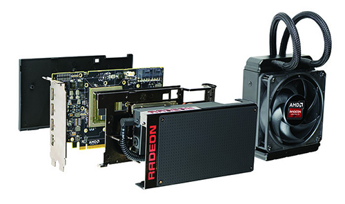
AMD R9 Fury X
Date issued:
Since the launch of the NVIDIA GTX Titan X and GTX 980 Ti graphics cards consumers have been waiting avidly for AMD's high-end response. After some wait AMD has introduced its new flagship Radeon R9 Fury X that is aimed at taking the fight to Nvidia's aforementioned GM200-based flagship graphics cards.
The AMD R9 Fury X is based on a new 'Fiji' GPU which makes use of AMD's existing GCN architecture and a number of modifications to improve efficiency and performance characteristics compared to earlier revisions of GCN. AMD, in that regard, takes a different strategy by choosing to work with an existing architecture in comparison to Nvidia who transitioned from Kepler to its new, efficiency-focused Maxwell architecture.
Radeon R9 Fury X |
Radeon R9 390X |
Radeon R9 290X |
GeForce GTX Titan X |
GeForce GTX 980 Ti |
GeForce GTX 980 |
|
| Launch date | June 2015 |
June 2015 |
October 2013 |
March 2015 |
June 2015 |
September 2014 |
| Codename | Fiji XT |
Grenada XT |
Hawaii XT |
GM200 |
GM200 |
GM204 |
| DX support | 12.0 |
12.0 |
12.0 |
12.1 |
12.1 |
12.1 |
| Process (nm) | 28 |
28 |
28 |
28 |
28 |
28 |
| Transistors (mn) | 8,900 |
6,200 |
6,200 |
8,000 |
8,000 |
5,200 |
| Approx Die Size (mm²) | 596 |
438 |
438 |
601 |
601 |
398 |
| Full implementation of die | Yes |
Yes |
Yes |
Yes |
No |
Yes |
| Processors | 4,096 |
2,816 |
2,816 |
3,072 |
2,816 |
2,048 |
| Texture Units | 256 |
176 |
176 |
192 |
172 |
128 |
| ROP Units | 64 |
64 |
64 |
96 |
96 |
64 |
| Peak GPU Clock/Boost (MHz) | 1,050 |
1,050 |
1,000 |
1,076 |
1,076 |
1,216 |
| Peak GFLOPS (SP) | 8,602 |
5,914 |
5,632 |
6,611 |
6,060 |
4,981 |
| Peak GFLOPS (DP) | 537 |
739 |
704 |
207 |
189 |
156 |
| Memory Clock (MHz) | 1,000 |
6,000 |
5,000 |
7,012 |
7,012 |
7,012 |
| Memory Bus (bits) | 4,096 |
512 |
512 |
384 |
384 |
256 |
| Max bandwidth (GB/s) | 512 |
384 |
320 |
336 |
336 |
224 |
| Default memory size (MB) | 4,096 |
8,192 |
4,096 |
12,288 |
6,144 |
4,096 |
| Memory type | HBM |
GDDR5 |
GDDR5 |
GDDR5 |
GDDR5 |
GDDR5 |
| Power Connectors | 8+8-pin |
8+6-pin |
8+6-pin |
8+6-pin |
8+6-pin |
6+6-pin |
| TDP (watts) | 275 |
275 |
290 |
250 |
250 |
165 |
| GFLOPS per watt | 31.28 |
21.50 |
19.42 |
26.44 |
24.24 |
30.19 |
| Current price (Newegg) | $649 |
$429 |
$329 |
$999 |
$649 |
$499 |
Increasing the core count
AMD's Radeon R9 Fury X uses the full implementation of the Fiji that includes 4,096 cores built on AMD's 28nm GCN architecture. For reference, AMD's GCN design has been in existence since December 2011 when the company launched the Radeon HD 7970, but this particular revision, GCN 1.2, was first found in the AMD Radeon R9 285 in 2014. GCN 1.2 is the third iteration of AMD GCN that features enhancements in the form of an improved geometry and tessellation setup as well as improved memory bandwidth by utilising lossless colour compression.
The previous-generation flagship R9 290X, and revised R9 390X, both feature 2,816 cores split over 11 compute units (CUs). The Fiji GPU found in R9 Fury X increases this to 16 CUs, resulting in 4,096 total cores and 256 texture units (TUs) given that there are 256 cores and 16 TUs per CU. The reference clock speed of 1,050MHz for the R9 Fury X translates into a staggering 8.6 TFLOPs of compute performance, the largest yet for a single-GPU AMD graphics card.
In terms of die size the 596mm² of Fiji is a hair smaller than Nvidia's Maxwell GM200, the full implementation of which is found on the GTX Titan X. AMD opts for a different distribution of space on Fiji, compared to Nvidia's GM200, choosing to dedicate the majority of the area to the compute power afforded by so many shader units.
Despite an increased number of compute units the number of render output units (ROPs) is maintained at 64 along with the same four geometry processors and associated hardware found in Hawaii, the GPU that powered the R9 290X. Another interesting note is the silicon required to maintain fast double-precision is omitted with Fiji; it can process double-precision at 1/16th of single precision which is slower than the previous-generation R9 290X.
At an architectural level games that rely heavily on geometry and simple operations may find the R9 Fury X's architecture to be a tad skewed, games that rely on the GPU's ability to shade pixels will fare much better. In predicting where the GPU bottlenecks of the future may lie AMD and Nvidia have clearly chosen different strategies, Nvidia's GM200 is focused on a strong back-end while AMD's Fiji opts for a monstrous number of shaders.
Power consumption tweaks
AMD achieves a significant boost in the core count while maintaining a higher clock speed and yet it manages to do this while maintaining a TDP of 275W, similar to previous-generation parts. AMD has been able to achieve this impressive engineering feat by enacting a number of significant tweaks to the R9 Fury X.
Firstly, AMD has repurposed some of its knowledge from the Carrizo APUs to improve Fiji. More specifically, the company has implemented a better power-gating technique (SVI2) to save power when parts of the GPU aren't being used. This is also helped by more advanced power management that considers a wider variety of boost frequency and voltage combinations as well as temperature and silicon quality to maximise performance with the minimum required voltage. This technique, which is similar to what Nvidia deploys in GPU Boost, has a downside in that there is more card-to-card variation.
A second significant improvement in the realm of power consumptions comes with respect to the cooling solution deployed. By utilising watercooling as standard AMD is able to maintain lower GPU temperatures and, resultantly, lower power consumption - this happens because lower temperatures minimise power leakage. The last piece of the power consumption puzzle is High-Bandwidth Memory (HBM) which significantly lowers video memory power consumption compared to GDDR5.
High Bandwidth Memory - HBM
HBM is the next significant step for graphics card memory and it offers a number of benefits compared to GDDR5 such as lower power consumption, a wider memory bus, more memory bandwidth and lower-latency access. HBM does this by vertically stacking DRAM chips on top of each other directly on the GPU package, rather than placing them around the GPU on the graphics card PCB. All these DRAM chips connect to each other by through-silicon vias (TSVs) and use an interposer to connect to the GPU die.
In current generation HBM 1,024 TSVs go through each of the four HBM memory stacks providing a total of 1,024Gbps of memory bandwidth per stack, or 4,096Gbps in total for all four. This results in 512GB/s of total memory bandwidth, measured in the conventional way, which gives the R9 Fury X significantly more bandwidth than any other single-GPU graphics card on the market.
Those same HBM memory stacks may have significantly more bandwidth but they are also limited in capacity, at least for the first generation, which is why AMD's R9 Fury X ships with 4GB of video memory rather than something larger, like the 8GB AMD has endowed the R9 390X with. Each of the four stacks is comprised of four 256MB layers, meaning 1GB per stack and 4GB in total from the sum of the four stacks.
AMD claims that the 4GB frame-buffer is plenty enough for current PC gaming, even at 4K. To get around the lower memory availability AMD has improved the memory management methods in the graphics driver to make the most efficient use of the memory. In short, whether or not 4GB is enough is difficult to ascertain without a side-by-side comparison of a 4GB and 8GB R9 Fury X.
Performance and Overclocking
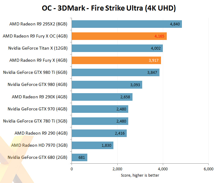
As a graphics card primed for 4K gaming the AMD Radeon R9 Fury X holds its own against Nvidia's similarly priced GTX 980 Ti and the much more expensive GTX Titan X. Performance, on the whole, is neck-and-neck with Nvidia's GTX 980 Ti, with the two cards trading blows depending on the resolution and the specific game title at hand.
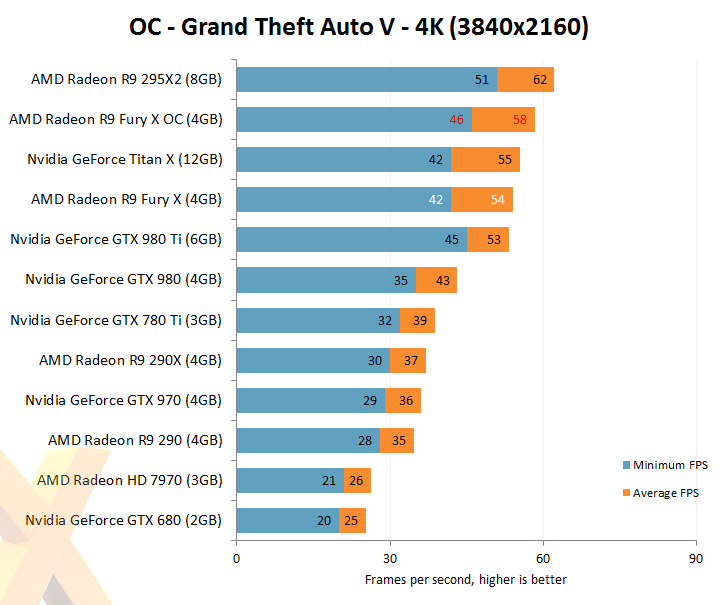
Looking at overclocked performance and the R9 Fury X has a modest amount of overclocking potential, enough to see it edge past the stock Nvidia GTX Titan X graphics card.
Even with AMD's best efforts to tame power consumption of the R9 Fury X using a myriad of tweaks the new AMD GPU is the most power-hungry flagship of the current generation, consuming about 30W more than Nvidia's GM200-based solutions.
Summary
With the R9 Fury X AMD has been able to create a flagship graphics card capable of trading blows with Nvidia's GTX 980 Ti and GTX Titan X in the 4K gaming arena. At a price point of $649 the R9 Fury X delivers competitive gaming performance, innovative HBM memory and a high-quality watercooling solution.