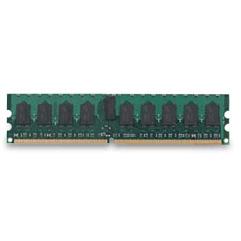
Hynix 1GB DDR3 PC3-8500 (1066) Single Channel Server Memory
Scan code: LN27472
Manufacturer code: HMT112U7AFP8C-G7T0
End Of Life
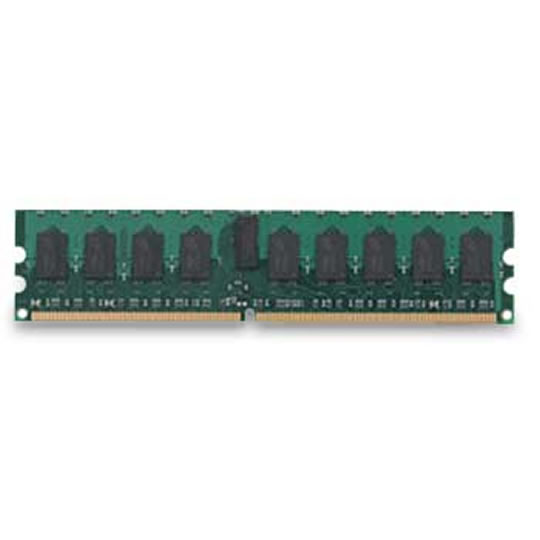

Hynix 1GB DDR3 PC3-8500 (1066) Single Channel Server Memory
1GB Hynix Server Memory, DDR3, PC3-8500 (1066MHz), 240 Pin, ECC, Unbuffered, CAS 7-7-7
Scan code:
LN27472
Manufacturer code:
HMT112U7AFP8C-G7T0
This product is no longer available to purchase.
Email me when the availability or price changes
Product Overview
This Hynix unbuffered Dual In-Line Memory Module(DIMM) series consists of 1Gb A version. DDR3 SDRAMs in Fine Ball Grid Array(FBGA) packages on a 240 pin glass-epoxy substrate. This DDR3 Unbuffered DIMM series based on 1Gb A ver. provide a high performance 8 byte interface in 133.35mm width form factor of industry standard. It is suitable for easy interchange and addition.
Features
• VDD=VDDQ=1.5V
• VDDSPD=3.3V to 3.6V
• Fully differential clock inputs (CK, /CK) operation
• Differential Data Strobe (DQS, /DQS)
• On chip DLL align DQ, DQS and /DQS transition with CK transition
• DM masks write data-in at the both rising and falling edges of the data strobe
• All addresses and control inputs except data, data strobes and data masks latched on the rising edges of the clock
• Programmable burst length 4/8 with both nibble sequential and interleave mode
• BL switch on the fly
• 8banks
• 8K refresh cycles /64ms
• DDR3 SDRAM Package : JEDEC standard 82ball FBGA(x4/x8) , 100ball FBGA(x16) with support balls
• Driver strength selected by EMRS
• Dynamic On Die Termination supported
• Asynchronous RESET pin supported
• ZQ calibration supported
• TDQS (Termination Data Strobe) supported (x8 only)
• Write Levelization supported
• Auto Self Refresh supported
• 8 bit pre-fetch


