Our Aim
To provide you with an overview on New And existing technologies, hopefully helping you understand the changes in the technology. Together with the overviews we hope to bring topical issues to light from a series of independent reviewers saving you the time And hassle of fact finding over the web.
We will over time provide you with quality content which you can browse and subscribe to at your leisure.
TekSpek 's

NVIDIA GeForce GTX 980 & 970 High End Maxwell 28nm
Date issued:
High-end Maxwell
With the launch of the new GeForce GTX 980 and GTX 970 graphics cards Nvidia is rolling out the latest Maxwell architecture to its high-end desktop graphics cards. Prior to this release Maxwell had been limited to the entry-level GTX 750 Ti and a handful of mobile GeForce GPUs.
Both the GTX 980 and GTX 970 make use of the GM204 GPU, and Nvidia is still to release the architecture-topping GM210. The GM204 GPU, therefore, isn't going to provide a quantum leap over existing GTX 700-series GPUs. However, the introduction of the GTX 980 and 970 makes a lot of sense for consumers and, crucially, for Nvidia.
The new Maxwell duo have triggered the phasing-out of the older GTX 780 Ti, GTX 780 and GTX 770 due to the noticeably better performance, lower power consumption and greatly reduced manufacturing cost on offer. Yet more impressive is the fact Nvidia can bring these new GPUs to market at a lower cost than Kepler equivalents. The GTX 980's introductory $549 MSRP is a sizeable reduction from the $699 the GTX 780 Ti commanded during its launch.
Nvidia GeForce GTX 980 (4GB) |
Nvidia GeForce GTX 970 (4GB)* |
Nvidia GeForce GTX 780 (3GB) |
Nvidia GeForce GTX 680 (2GB) |
AMD Radeon R9 290X (4GB) |
AMD Radeon R9 290 (4GB) |
|
| Launch date | September 2014 |
September 2014 |
May 2013 |
March 2012 |
October 2013 |
November 2013 |
| Codename | GM204 |
GM204 |
GK110 |
GK104 |
Tahiti |
Tahiti |
| DX API | 11.2 |
11.2 |
11.2 |
11.2 |
11.2 |
11.2 |
| Process (nm) | 28 |
28 |
28 |
28 |
28 |
28 |
| Transistors (mn) | 5,200 |
5,200 |
7,100 |
3,540 |
6,200 |
6,200 |
| Approx Die Size (mm²) | 398 |
398 |
551 |
294 |
438 |
438 |
| Full implementation of die | Yes |
No |
No |
Yes |
Yes |
No |
| SM Units | 16 |
13 |
13 |
8 |
NA |
NA |
| Processors | 2,048 |
1,664 |
2,304 |
1,536 |
2,816 |
2,560 |
| Texture Units | 128 |
104 |
192 |
128 |
176 |
160 |
| ROP Units | 64 |
56 |
48 |
32 |
64 |
64 |
| Peak GPU Clock/Boost (MHz) | 1,216 |
1,178 |
900 |
1,058 |
1,000 |
947 |
| Peak GFLOPS (SP) | 4,981 |
3,920 |
4,147 |
3,250 |
5,632 |
4,849 |
| Peak GFLOPS (DP) | 156 |
122 |
173 |
135 |
704 |
606 |
| Memory Clock (MHz) | 7,012 |
7,012 |
6,008 |
6,008 |
5,000 |
5,000 |
| Memory Bus (bits) | 256 |
256 |
384 |
256 |
512 |
512 |
| Max bandwidth (GB/s) | 224 |
224* |
288 |
192 |
320 |
320 |
| Power Connectors | 6+6-pin |
6+6-pin |
8+6-pin |
6+6-pin |
8+6-pin |
8+6-pin |
| TDP (watts) | 165 |
145 |
250 |
195 |
250 |
250 |
| GFLOPS per watt | 30.19 |
27.03 |
16.59 |
16.66 |
22.52 |
19.40 |
| Current price (Newegg) | $549 |
$329 |
$420 |
NA |
$460 |
$370 |
The flagship GeForce GTX 980
The flagship graphics card built from the new GM204 GPU is the GeForce GTX 980. Equipping the full physical capability of the GM204 die the GTX 980 still makes use of the current 28nm process. Compared to GTX 780 it replaces, and AMD's best offering, the R9 290X, the GTX 980 is 28 per cent and 9 per cent smaller, respectively. A smaller die usually means less power consumption and lower cost.
Relative to its GTX 700 series namesake, the GTX 780, the new Maxwell flagship, features 11 per cent fewer shading cores, 33 per cent fewer texture units, a 50 per cent narrower memory bus and 34 per cent less power consumption. All those deductions end up with the GTX 980 being a full 25 per cent faster than the GTX 780, so how does that work?
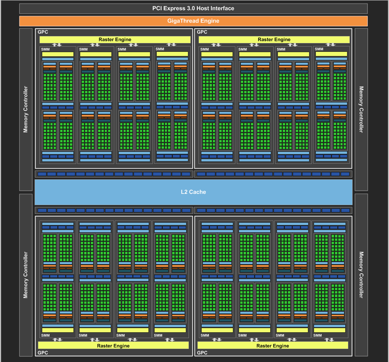
The full GM204 implementation
Maxwell's efficiency
The Maxwell GM204 GPU achieves notable performance wins compared to its predecessor due to an array of efficiency tweaks. These tweaks extend all the way to the building blocks of the Maxwell architecture. Each graphics processing cluster (GPC) in Maxwell has 512 processing cores, compared to 576 on Kepler. Phrased another way, that's 128 cores per streaming multiprocessor (SM), down from 192 in the Kepler architecture.
Reducing the number of cores in each SM, thus reducing the total number of cores in a GPC, allows Nvidia to reduce power consumption. This efficiency increase occurs since the SM scheduler is more effective at dealing with 128 cores efficiently, rather than 192. Some further efficiency gains are made by offsetting parts of the scheduling process to the GeForce driver. The end result of reconfiguring the layout of cores and SMs is that each individual Maxwell core is capable of 1.4x the performance of Kepler. In product terms, the 2,048 Maxwell cores on the GTX 980 is worth the same as the 2,880 Kepler cores on the GTX 780 Ti.
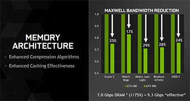
While most of Maxwell's design has entailed a more efficient organisation of fewer hardware components, some areas have been bolstered. The number of render outputs (ROPs) has been doubled from 32 to 64, particularly since a lack of ROPs proved limiting on previous-generation cards. Anticipating future growth in high-resolution gaming Nvidia has also upped the frame buffer from 3GB to 4GB of GDDR5. Continuing along the memory pathway Nvidia has balanced-out the 50 per cent reduction in the width of the memory bus by bolstering the GPU's L2 cache from 512KB to 2,048KB, thus reducing the frequency of memory access requests.
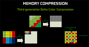
Another trick around the narrower memory bus is deployed with respect to colour compression. Using refined algorithms and a third-generation delta compression engine the Maxwell GPU is able to effectively determine when less data needs to be written across the memory bus. Maxwell is able to reduce memory transactions by approximately 25 per cent making its 7Gbps memory frequency akin to 9.3Gbps in reality.
 |
 |
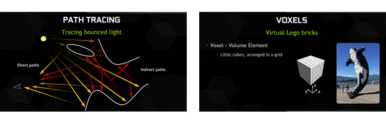
A last interesting addition to the Maxwell architecture covers methods of producing accurate lighting. Using an Nvidia-developed method called 'Voxel Cone Tracing' (VCT) the Maxwell GPU features 3x faster global illumination compared to previous-generation equivalents. This provides the foundations for real-time VCT and, if game developers make use of the technology, near-perfect global illumination. Relative to what's already available the VCT technique to dynamic lighting is a halfway house between SSAO and true path-tracing.
 |
GeForce GTX 970: a smaller chip off the bigger block
While the headlining GeForce GTX 980 will appeal to performance junkies and deep-walleted enthusiasts, it's the GTX 970 that will capture the attention of most buyers. In many ways the GTX 970 is hardly different from its bigger brother. The main difference is the removal of three SM units, giving the GTX 970 13 compared to the GTX 980's 16. The number of cores and texture units take a tumble to 1,664 and 104, respectively, as a result of this reduction.
To dampen the performance of the GTX 970 a little further, Nvidia takes the peak boost clock down from 1,216MHz to 1,178MHz. The backend of the GTX 970 remains identical with the same frequency and amount of memory. Overall it would be reasonable to infer that stock-vs.-stock the GTX 970 is around 15 per cent slower than the GTX 980.
Fewer cores and a lower clock speed does also mean less power consumption. As if the 165W TDP of the GTX 980 wasn't already impressive enough, the GTX 970 is graced with a 145W TDP. At a price of $329 Nvidia knows the GTX 970 is going to pile the pressure on to AMD's R9 290X and R9 290. The company has already been aggressively price-cutting its Radeon R9 series parts but given that Nvidia can produce its GTX 970 fairly cheaply, AMD could struggle to remain competitive.
*But there is a key difference that could have an impact for future games. While the GeForce GTX 970 does indeed have a full 4GB of video memory, just like the GTX 980, the memory does not run at full speed at all times.
In particular, 3.5GB of the 4GB memory runs at full speed while the remaining 0.5GB runs at one-eighth of maximum speed. This is only important once the games engine requests more than 3.5GB of memory, which is rare, but the reason for this is how Nvidia has designed the GPU. Reducing this last portion of memory speed enables Nvidia to selectively switch off other related parts of the GPU, without having too much of an impact on performance, in order to hit a lower price point.
Performance
3DMark is the latest version of the hugely-popular synthetic benchmark series making use of DX11 features such as tessellation, compute shaders and multi-threading. This benchmark provides a modern assessment of a graphics card's capabilities in conditions that simulate current gaming titles.
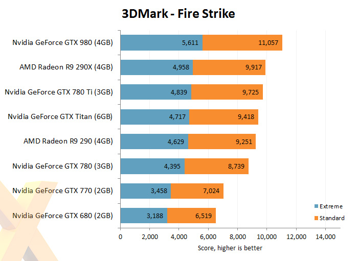
We've already seen why the Maxwell-powered GTX 980 is able to deliver more than its paper-based specification imply. Combining all Nvidia's architectural tweaks the GTX 980 delivers considerably more performance than every other single-GPU graphics card on the market. The claim the 2,048 Maxwell cores behave like 2,880 Kepler cores seems like a conservative one.
If you haven't upgraded your GPU since the GTX 680's release, two-and-a-half years ago, then you might be surprised to know the GeForce GTX 980 offers almost 70 per cent more performance.
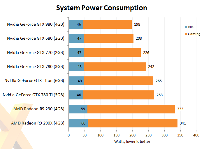
Even more impressive is that the GTX 980 consumes marginally less power than the GTX 680, and shaves a considerable 60W off power consumption of the GTX Titan and GTX 780 Ti. Worryingly for AMD is the fact its flagship Radeon R9 290X consumes over 70 per cent more juice while offering less graphics performance.
Summary
The Maxwell-powered GeForce GTX 980 and GTX 970 graphics cards underpin the saying that less is more. For a lower cost and smaller power budget than Kepler predecessors the Maxwell duo offer exceptional performance-per-watt characteristics. The GeForce GTX 970 and GTX 980 have redefined Nvidia's high-end GeForce offerings for the coming months.
Scan Computers is proud to retail the largest selection of Nvidia GeForce GTX 980 graphics cards in the UK. Please head on over to here to peruse our listings.