Our Aim
To provide you with an overview on New And existing technologies, hopefully helping you understand the changes in the technology. Together with the overviews we hope to bring topical issues to light from a series of independent reviewers saving you the time And hassle of fact finding over the web.
We will over time provide you with quality content which you can browse and subscribe to at your leisure.
TekSpek 's

Intel Core i5 6600K and Core i7 6700K
Date issued:
Intel generally follows a tick-tock philosophy for new processor launches. The tick represents a shrinking of the manufacturing process - 32nm to 22nm, for example - while the tock is indicative of a new architecture based on the leading process of that time. This has been the case since 2007.
A tick-tock approach is necessary to mitigate the risks introduced by switching to a smaller, more efficient manufacturing process and new architecture at the same time. The latest incarnation of this philosophy is the move from fifth-generation Core (Broadwell, tick) to sixth-generation Core (Skylake, tock), but what's new this time around is that Intel has introduced them so close together, with both microarchitectures available in desktop form in the summer of 2015.
The reason for this rests with the problems Intel had in producing an efficient yield of the 14nm process present in both Broadwell and Skylake. That has been ironed out now so Skylake becomes the dominant technology from hereon in.
Skylake is the overall embodiment of a number of new technologies that make the new processors even more efficient than their predecessors. Putting Skylake into context, let's see how the two available processors - K-series chips for the overclocker and enthusiast - line up against various other microarchitectures from days gone by.
Desktop |
|||||||||||
|---|---|---|---|---|---|---|---|---|---|---|---|
Model |
Cores / Threads |
CPU Clock (GHz) |
Turbo Boost (GHz) |
Process |
Die Size |
Cache |
IGP |
IGP Clock (MHz) |
DDR Support (MHz) |
TDP |
Launch Price (US 1ku) |
| Skylake Core Processor Family (6th Generation, LGA1151) | |||||||||||
| Core i7-6700K | 4 / 8 |
4.0 |
4.2 |
14nm |
TBC |
8MB |
HD 530 |
1,150 |
Dual 2,133 (DDR4) |
91W |
$350 |
| Core i5-6600K | 4 / 4 |
3.5 |
3.9 |
14nm |
TBC |
6MB |
HD 530 |
1,150 |
Dual 2,133 (DDR4) |
91W |
$243 |
| Broadwell Core Processor Family (5th Generation, LGA1150) | |||||||||||
| Core i7-5775C | 4 / 8 |
3.3 |
3.7 |
14nm |
TBC |
6MB |
Iris Pro 6200 |
1,150 |
Dual 1,600 |
65W |
$366 |
| Core i5-5675C | 4 / 4 |
3.3 |
3.8 |
14nm |
TBC |
4MB |
Iris Pro 6200 |
1,100 |
Dual 1,600 |
65W |
$276 |
| Haswell Core Processor Family (4th Generation, LGA1150) | |||||||||||
| Core i7-4790K | 4 / 8 |
4.0 |
4.4 |
22nm |
177mm² |
8MB |
HD 4600 |
1,250 |
Dual 1,600 |
84W |
$339 |
| Core i7-4770K | 4 / 8 |
3.5 |
3.9 |
22nm |
177mm² |
8MB |
HD 4600 |
1,250 |
Dual 1,600 |
84W |
$339 |
| Core i5-4690K | 4 / 4 |
3.5 |
3.9 |
22nm |
177mm² |
6MB |
HD 4600 |
1,200 |
Dual 1,600 |
84W |
$242 |
| Core i5-4670K | 4 / 4 |
3.4 |
3.8 |
22nm |
177mm² |
6MB |
HD 4600 |
1,200 |
Dual 1,600 |
84W |
$242 |
| Ivy Bridge Core Processor Family (3rd Generation, LGA1155) | |||||||||||
| Core i7-3770K | 4 / 8 |
3.5 |
3.9 |
22nm |
160mm² |
8MB |
HD 4000 |
1,150 |
Dual 1,600 |
77W |
$313 |
| Core i5-3570K | 4 / 4 |
3.4 |
3.8 |
22nm |
160mm² |
6MB |
HD 4000 |
1,150 |
Dual 1,600 |
77W |
$212 |
| Sandy Bridge Core Processor Family (2nd Generation, LGA1155) | |||||||||||
| Core i7-2700K | 4 / 8 |
3.5 |
3.9 |
32nm |
216mm² |
8MB |
HD 3000 |
1,350 |
Dual 1,333 |
95W |
$332 |
| Core i7-2600K | 4 / 8 |
3.4 |
3.8 |
32nm |
216mm² |
8MB |
HD 3000 |
1,350 |
Dual 1,333 |
95W |
$317 |
| Core i5-2500K | 4 / 4 |
3.3 |
3.7 |
32nm |
216mm² |
6MB |
HD 3000 |
1,100 |
Dual 1,333 |
95W |
$216 |
Intel continues to segregate the Core i7 and Core i5 chips through the use of hyperthreading. The Skylake-infused Core i7-6700K utilises four cores and eight threads for maximum performance, much like the Broadwell, Haswell, Ivy Bridge and Sandy Bridge designs previously. Frequencies are generally the same, too, so extra performance is generally down to improvements in processing, and we'll come to those in a moment. The Core i5-6660K, meanwhile, follows a similar tack, with frequencies that are very similar to previous chips at the same rung in Intel's desktop ladder.
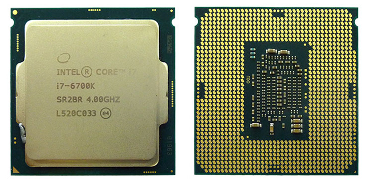
Different form factor but the same packaging style as previous Core chips.
Architecture improvements - CPU
So what has Intel done in order to improve performance per MHz? Skylake, compared to previous Intel microarchitectures, has a number of technologies that combine to improve this all-important IPC by around 10 per cent in best-case scenarios.
First off, Skylake can process more information in each cycle through enhanced parallelism. Key performance drivers such as the out-of-order window, in-flight stores, loads, scheduled entries, and both integer and floating-point files have been improved markedly when compared to Haswell. The front-end branch predictor has been privy to a redesign for better performance while deeper buffers help to ensure that all instruction traffic is processed efficiently.
And it's this incremental improvement theme that plays large in Skylake - the architecture isn't a ground-up design of what's gone before. Rather, it's Intel's engineers looking at the portions of previous architectures that weren't quite as polished as they could have been and rectifying those: this is evolution rather than revolution.
Overall chip latencies have been reduced, as well, because there's now more granular power gating to ensure that parts of the CPU core power down when more quickly when not in use.
But it's not all about core improvements. Intel also spent time in optimising the chip's cache to be more efficient. It says the last-level cache is now twice as good at weeding out missed hits than on, say, Broadwell, and Skylake can now use eDRAM memory, previously reserved for graphics alone, as an additional cache as and when needed.
Skylake jumps to its fastest frequency far more quickly than previous Intel architectures thanks to Speed Shift technology where the processor, installed on a compatible operating system such as Windows 10, can switch what are known as P-states 30x faster than before. Getting up to maximum speed and then powering down helps pure performance and energy efficiency in one fell swoop.
For the first time in recent history, Intel has two distinct variations of the Skylake technology designed for consumers (Core) and workstation/server (Xeon) respectively. While different, and Xeon details are yet to be disclosed, Intel understands the need to beef-up the security aspects of the latest processors.
That's where Intel Software Guard Extensions (SGX) and Memory Protection Extensions (MPX) come into play. SGX works by creating dedicated, secure enclaves for code to run on such that they cannot be breached by the operating system kernel or hypervisor. The purpose is to create an area where even a compromised, attacked OS cannot read nor write pages existing within the enclave.
The clever part is that multiple enclaves can be created. MPX, meanwhile, locks down one of the simplest, oldest attacks known as stack buffer overflow where malicious code is injected after the stack is corrupted through targetted overflow. MPX mitigates overflow by ensuring that a program cannot write more to a buffer than what space has been allocated to it.
Skylake CPUs are therefore more efficient and more secure than any previous core processors.
Architecture improvements - GPU
There are changes afoot in the GPU side, too. Skylake uses the slice/unslice/subslice hierarchy from previous Intel HD Graphics but expands upon them to build a bigger, faster GPU. The fastest implementation of the graphics, known as Iris Pro, can use up to 72 execution units, up from 40 on the Haswell core. What's more, they're now DX12, Open CL 2.0 and Open GL 4.4 compliant and can offer a potential 1.15GFLOPS of performance which is equivalent to a mainstream discrete graphics card from 2015.
Just like the CPU, there are improvements in general processing ability through a clean-up of the architecture. Intel cites meaningful gains for vertex and geometry processing while energy efficiency is further improved by Skylake now having the ability to power down the unslice section independently from the slice. As you would expect, other general improvements include better pixel and fill-rate performance, more efficient implementation of anti-aliasing, improved colour compression and larger cache sizes.
Intel, it seems, has taken a look at what AMD and Nvidia are doing in the discrete graphics space and taken the best options for Skylake. But it's not all about the shading cores for Skylake's graphics. Intel has improved the Quick Sync video function in terms of power usage, now supports the processing of 4K60 RAW video, and had dedicated hardware for the next generation of compression codecs such as H.265, which is now accelerated for both decode and encode.
Understanding that Skylake is designed to fit into premium tablets and all the way up to high-performance desktop, Intel now includes a dedicated image signal processor right on the die. It supports up to four cameras - two in concurrent usage - and sensors up to 13MP. Aimed more at the mobile segment, Intel hopes the integration will reduce the time to market for devices featuring the company's technology.
Architecture improvements - platform
Coming back to high-end desktop, what we do know is that Skylake is presented in a different form factor known as LGA1151. This is important because it denotes both a socket change and consequently a slew of new motherboards based on the Z170 chipset.
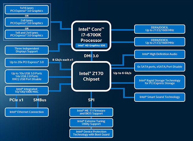
A bump in specification for the chipset
The pertinent points are that Skylake processors use either dual-channel DDR3L memory or DDR4 memory at up to 2,133MHz speeds and offer more granular overclocking than ever before; Intel says that enthusiasts can overclock the unlocked Core i7-6700K in 1MHz base-clock increments.
A standard 16 PCIe 3.0 lanes are still attributed to the graphics, split in the same way as Z97, but it's interesting what Intel has done with the expansion capability of the Z170. Z97, if you remember, had an additional 8 PCIe 2.0 lanes attached to the chipset; some motherboard manufacturers used them to include PCIe x1 slots and various high-speed peripherals, but most ran into difficulties when catering for super-fast storage that required multiple lanes on its own.
Intel realised this and now increases the chipset-based PCIe lanes to 20 Gen 3.0, and this means that motherboard guys don't need to worry about housing and routing the latest generation of M.2 solid-state drives - Intel has finally taken the lane arbitration issue away. We expect to see boards with multiple M.2 slots each capable of x4 PCIe 3.0 bandwidth.
Appreciating that the chipset now needs to communicate with the processor through a faster link due to more traffic generated via the enhanced PCIe lanes, the Direct Media Interface (DMI) is upgraded to 3.0, promising speeds of up to 8GT/s. In other news, Intel ups the USB 3.0 complement to 10 ports, instead of six on Z97, but there's no chipset room for USB 3.1.
Skylake: more than just a new CPU
Let's be clear. Those investing in the Skylake K-series platform need to purchase the processor, LGA1151-based Z170 motherboard and DDR4 memory in one fell swoop. The platform will be more expensive than, say, Haswell because the Skylake motherboards and DDR4 memory attract a reasonable price premium. The good news is that you can reuse any recent Intel-specific cooling because motherboards feature the same mounting holes.
Other Skylake-based chips will fill out the sixth-generation Core portfolio in Q3 2015, according to Intel, though early adopters are limited to just these aforementioned two. For those who appreciate the key new technologies and want the most advanced Intel consumer platform to date should look at the new Skylake architecture first and foremost. As always, Scan Computers has the widest range of Intel Skylake CPUs and motherboards available.